
AtaiTec 公司的成立是為了幫助高速電路設計的工程師提高效率來執行他們其日常訊號完整度 (Signal Integrity, SI) 的任務
1.2D/3D field solver simulation
2.Circuit simulation
3.Channel simulation
4.VNA/TDR measurements
5.Correlation and ...etc.
Atatec提供了甚麼解決方案 ?
我們專注於IC,封裝,連接器,電纜和電路板的信號和電源完整性建模,仿真和測量的相關性。 我們的類移動應用程序的信號和電源完整度軟件, 一起完善了您的3D全波場求解器,電路模擬器和向量分析,並幫助您關聯仿真和測量結果:
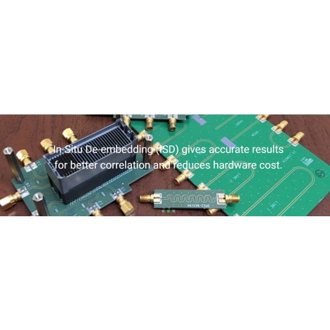
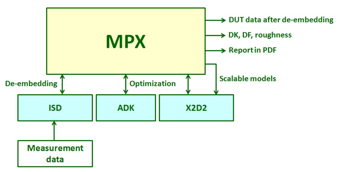
- ISD (or in Situ De-embedding) is meant to replace TRL calibration and help save SMAs and board material.
- ADK (or Advanced SI Design Kits) is a collection of many commonly used SI utilities that provide a one-stop solution for your SI analysis needs.
- X2D2 is an ultra accurate 2D RLGC field solver with surface roughness model to help you define the PCB stackup and trace width/spacing for impedance control and desired insertion loss.
- MPX (or Material Property Extractor) automates de-embedding, PCB material property extraction and report generation into just one mouse click.
為何Ataitec是獨特的 ?
我們需要了解以下方面的基本知識和局限性:
- Boundary element method (BEM),
- Finite element method (FEM),
- Modified nodal analysis (MNA),
- Calibration methods (SOLT, TRL, unknown thru), etc.
Ataitec軟體解決了甚麼樣的問題 :
- How do you set up models, excitation, and boundary conditions for 3D full-wave solvers?
- How much error are you getting from the simulation or measurement data?
Ataitec軟體提供了甚麼樣的效益 ?
- 極佳的投報率 (ROI) : Want to know how you can save SMAs, board material, and time in VNA measurements? Just try our In Situ De-Embedding (ISD)
- 3周的試用期 : Just send us two Touchstone files — one for through trace and one for DUT + test fixture — and we will send you the extracted DUT Touchstone file.