

Skorpios 是一家半導體公司,基於其專有的晶圓級異構集成工藝(稱為 Tru-SiPh™)提供高度集成的產品。這種新穎的工藝利用現有的矽製造生態系統,以成熟的 CMOS 製造成本實現高帶寬互連。Skorpios 獨特的平台可用於處理廣泛的應用:用於網絡、雲計算、消費、醫療等的高速視頻、數據和語音通信。
公司位置 : SKHQ: Albuquerque, NM
- R&D, Product Design, G&A, M&S
- Module Manufacture, Test
- 47,500 SF with 10,000 SF Expansion Area
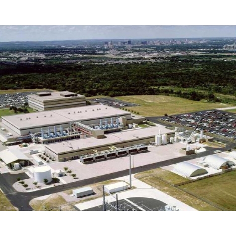
晶圓工廠 : SKTX: Austin, Texas
- 70,000 sq. ft Class-10 Clean Room
- Develop and Manufacture Skorpios’ Proprietary Heterogeneous Integrated Opto-Electronic Circuits
- Support Foundry Customer Services & Products
- >1000 Wafers per Month Capacity

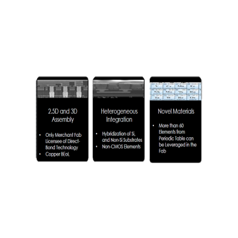
Skorpios Enabling Technologies :
.png)
Tru-SiPhTM 的優勢 :
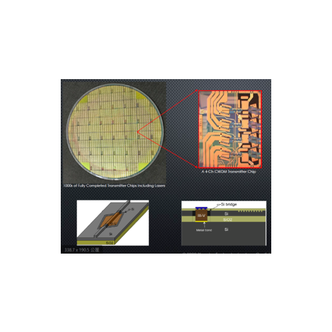
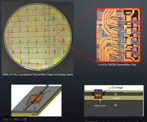
1. Skorpios Heterogeneous Si Photonics
- We Combine Different Material Systems on the Same Chip
- III-V Material: Good for Lasers, Modulators, Photodetectors, SOAs
- Si/SiO2: Good for All Passive Devices
- We Integrate All Optical Devices on A Single Chip
- CMOS Fab on 8” Wafers
- Single Process Flow for All Lasers, Modulators, SOAs, PDs, and Tuning-Free Mux/DeMux
- Wafer-Level Laser Burn-in
- Wafer-Level Chip Testing
- No Complicated Assembly
- No Need for Chip Package
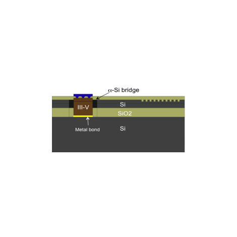
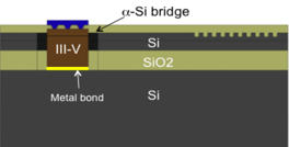
2. Skorpios Laser/SOA Have Lowest Thermal Impedance
- Ensured by Metal Bonding of Laser/SOA Directly onto the Si Substrate
- Allows Very Small Area of Lasers and SOAs
- Enables Densely Integrated Lasers and SOAs
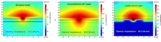
Skorpios Laser Size Is ~1/4 of Leader Brand Laser
– Consistent with Thermal Impedance
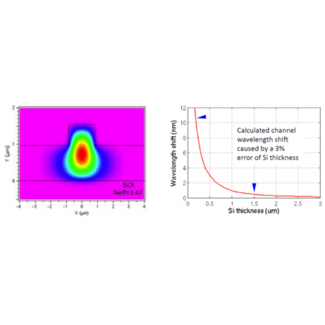
3. Thick-Si Platform
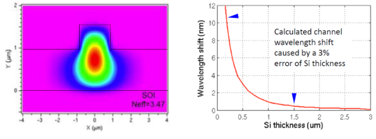
- Low Coupling Loss with Laser/SOA/EAM Waveguides (Similar Mode Sizes, Similar Effective Indices)
- Fabrication and Polarization Insensitive (Optical Mode Is Almost Completely Confined in the Si Layer)
- Waveguide Loss <0.5 dB/cm (Very Little Optical Mode Overlap with Si/SiO2 Interfaces)
- High Optical Power Handling Capability (Large Optical Mode)